SOLIDWORKS Electrical 2019 introduces some new features and enhancements to help you streamline your processes and work faster.
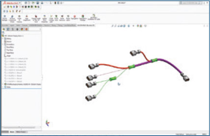
ENHANCED DYNAMIC CONNECTOR CONFIGURATION
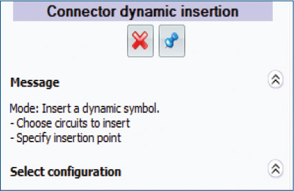
SOLIDWORKS Electrical 2019 introduces enhanced Dynamic connector insertion supporting graphical segmentation and mated connector pairs to streamline and simplify the insertion of segmented and mated connectors.
ENHANCED ABILITY TO CHANGE MEASUREMENT UNITS
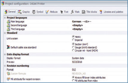
To streamline and simplify the way to define and change measurement units within the project, SOLIDWORKS Electrical 2019 allows you to easily change preferred measurement units. In the properties of wires, cables and manufacturer parts, you can choose to display the dimensions in millimeters or inches.
AUTO-GENERATED LINKS IN GENERATED REPORT DRAWINGS & EXPORTED PDF FILES
Enjoy streamlined navigation to BOM/report components in reports and PDF drawings:
- You can add go-to links for BOM/report components for generated reports. When you manage links in reports, they are automatically generated in the report drawings.
- You can export PDF files with go-to links for BOM/report components to navigate to generated PDF drawings.
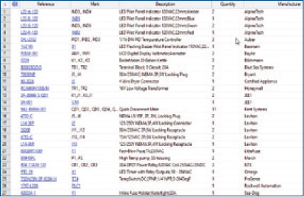
ENHANCED TABLES, BOM & DOC IN FLATTENED DRAWINGS
SOLIDWORKS Electrical 2019 auto-generates the proper and organized flattened route drawings and related tables. All information displayed in the tables like BOM, circuit summary and connector tables presented in Flattened route drawings per the schematic data, streamlining and simplifying ways to create tables and documentation for flattened documents based on schematic data.
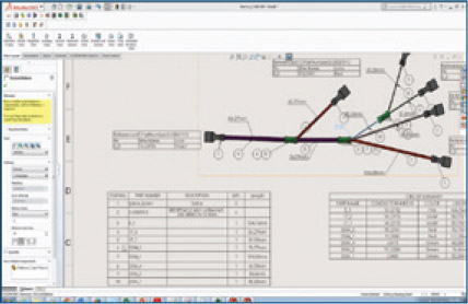
SPLICE IN SOLIDWORKS ELECTRICAL 3D
Effectively use splices from SOLIDWORKS® Electrical schematics, using a passing circuit symbol to represent a circuit with the same equipotential on both sides of the splice and bring that into 3D and route using the various auto-route options with effective flatten-route capability. This gives you the ability to use schematic-driven splices in 3D that can be flattened and documented via automated table creation.
PARTIAL OR FIXED LENGTH COVERINGS
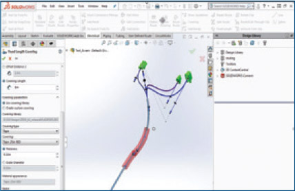
Effectively create partial or fixed length coverings for various locations and elements on the route segments, providing a streamlined and simplified way to create partial or fixed length coverings for Harness and inline features such as Cable socks and label tags (inline).
IPC NETLIST OUTPUT (SOLIDWORKS PCB)
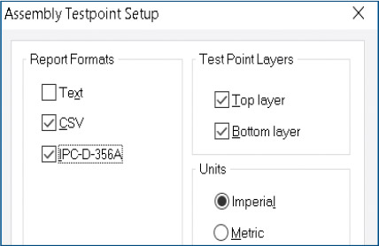
IPC netlist supplements Gerber output to provide, among other things, electrical connectivity information provided to the Printed Circuit Board (PCB) manufacturer as part of the fabrication package. Because Gerber lacks connectivity information, an IPC netlist helps the board house compare and validate that user-supplied Gerber data or Gerber data modified by the PCB manufacturer matches the source CAD design before fabrication.
MECHANICALLY-DRIVEN PCB PLACEMENT BARRIERS (SOLIDWORKS PCB)
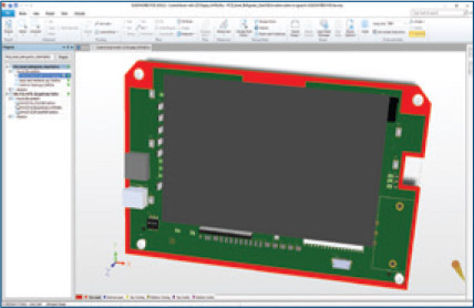
Any required placement restrictions of electronic components on the Printed Circuit Board (PCB) can be defined in SOLIDWORKS 3D CAD and passed through SOLIDWORKS PCB Connector to SOLIDWORKS® PCB. These placement restrictions can be applied to the surface of a PCB or offset to facilitate height restrictions. Any placement restrictions from 3D CAD will appear as placement barriers in SOLIDWORKS PCB.
SOLIDWORKS mechanical designers can electronically communicate, control and validate any required placement restrictions during the design phase to help ensure proper board and enclosure form and fit, and further streamline the ECAD-MCAD workflow.
COLLABORATION SUPPORT OF COMPONENT LOCK/FIX STATES AND FLIPPED CHANGES 3D ANNOTATIONS FOR ALL
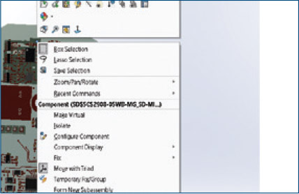
ECAD-MCAD collaboration through SOLIDWORKS PCB Connector has been enhanced to support the passing of electronic components’ locked/fix states as well as the ability to flip an electronic component from one side of the PCB to the other and collaborate that change in the z-axis.
This new feature adds a capability for SOLIDWORKS mechanical designers to modify electronic component locations in SOLIDWORKS 3D CAD and enables a greater level of control over electronic components desired location, preventing accidental changes during PCB layout.
COPPER VISUALIZATION (SOLIDWORKS PCB)
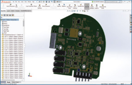
ECAD-MCAD collaboration through SOLIDWORKS PCB Connector has been enhanced to include the visualization of copper elements on a PCB in SOLIDWORKS 3D CAD.
SOLIDWORKS mechanical designers can now see copper traces and pads when modifying electronic component locations in SOLIDWORKS 3D CAD to aid in the decision making process when determining the best component location.
Share
Meet the Author
view all posts by GSC
SOLIDWORKS Webinars & Power Hours
